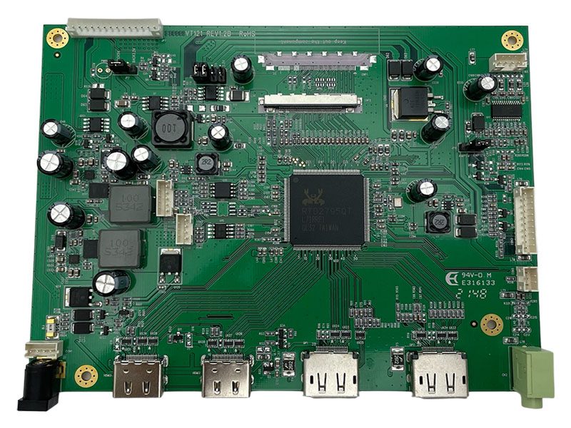
LCD Monitor Motherboard
Model:VT121
This LCD monitor motherboard is designed for high-resolution applications and includes the following features:
◎ The A/D Board is designed to connected with 4K x 2K TFT LCD panel, using the main chip manufactured by Realtek , including Color Engine and Audio DAC which can output high quality
picture and sound quality.
◎ It supports 8 pairs V-by-one and eDP interface for 4Kx2K Panel.
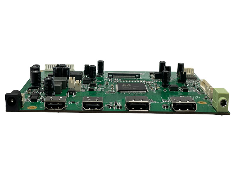
◎ The A/D Board Offers HDMI and DisplayPort to support input signal up to 4Kx2K 60Hz.
◎ Support Picture Rotate function.
◎ Built in10Wx2 audio amp.(Optional)
◎ In HDMI mode , the board supports color depth of 6-Bit , 8-bit , 10 bit and 12-bit.
◎ In DisplayPort mode , three link layer speed HBR2(5.4GHz) , HBR(2.7GHz) , RBR(1.6GHz) are supported.
◎ Wide input voltage range 12V ~ 24V
◎ Operating temperature range: 0℃ to +50℃
◎ Storage temperature range: -40℃ to +60℃
◎ Operating humidity range : 0% to 80% (Non-condensing)
◎ Storage humidity range : 0% to 80% (Non-condensing)
◎ RoHS compliant.
Download
Add to inquiry
◎ The A/D Board is designed to connected with 4K x 2K TFT LCD panel, using the main chip manufactured by Realtek , including Color Engine and Audio DAC which can output high quality
picture and sound quality.
◎ It supports 8 pairs V-by-one and eDP interface for 4Kx2K Panel.
◎ The A/D Board Offers HDMI and DisplayPort to support input signal up to 4Kx2K 60Hz.
◎ Support Picture Rotate function.
◎ Built in10Wx2 audio amp.(Optional)
◎ In HDMI mode , the board supports color depth of 6-Bit , 8-bit , 10 bit and 12-bit.
◎ In DisplayPort mode , three link layer speed HBR2(5.4GHz) , HBR(2.7GHz) , RBR(1.6GHz) are supported.
◎ Wide input voltage range 12V ~ 24V
◎ Operating temperature range: 0℃ to +50℃
◎ Storage temperature range: -40℃ to +60℃
◎ Operating humidity range : 0% to 80% (Non-condensing)
◎ Storage humidity range : 0% to 80% (Non-condensing)
◎ RoHS compliant.
Specification
A/D board option
| Mode | Teleview part no. | Description |
| 1 | C121A795A01-- | 2 HDMI+ 2 DP, Audio, V-by-one |
| 2 | C121A795A21-- | 2 HDMI+ 2 DP, Audio, eDP |
| 3 | C121P795A01-- | 2 HDMI+ 2 DP, Audio, V-by-one,W/power board |
Component Information
| -- | -- | -- | -- |
| I/O | Input | DisplayPort 1.2 | Display Port Connector × 1 |
| DisplayPort 1.2 | Display Port Connector × 1 | ||
| HDMI 2.0 | Type A 19Pin × 1 | ||
| HDMI 2.0 | Type A 19Pin × 1 | ||
| Key Pad | 5Key Tact Switch w/LED | ||
| Power | DC Jack2.5 | ||
| Audio | 3.5mm Audio Phone Jack | ||
| Output | Panel Interface | 41Pin / 0.5mm eDP Connector×1 | |
| Panel Interface | 51Pin / 0.5mm V-by-1 Connector×1 | ||
| Audio Speaker | Wafer 4Pin 2.0mm (R/L × 1) | ||
| Power | -- | Input Power | DC + 12V / +24V |
| Panel Power | DC +3.3V / +5V / +12V | ||
| Operate Mode | Normal / Stand By | ||
| Power Consumption |
Normal Mode<15W Stand By Mode |
||
| Others | -- | Audio AMP | 2 x 10W@8ohm 1Vrms THD:10% |
| OSD Control | Power, Menu, Exit, Up, Down | ||
| OSD Language | English (Added by Request) |
Timing Table
• The following table includes all display modes that this AD board can support; The product does not ensure proper operation if the display mode is not in the table.
• The table has covered most of popular display modes, especially VESA standard definition display modes. It is possible to add special display mode into the table if customer offers the timing information and verified successfully by us.
• Not every application can apply to all modes in the table . It depends on panel , resolution and some key parameters.
• Most panels does not support 75Hz vertical refresh rate while the A/D board can support . Improper application out of panel limit range may cause the damage to panel.
• The best display performance can be shown only when the input display mode matches the panel resolution.
| Video Mode | f H (kHz) | fV (Hz) | Dot clock (MHz) | HDMI 1.4 | HDMI 2.0 | DisplayPort 1.2 | ||
| VESA | 640x400 | 37.9 | 85 | 31.5 | - | - | - | |
| VGA 640x480 | 31.469 | 59.94 | 25.175 | O | O | O | ||
| 37.861 | 72.809 | 31.5 | O | O | O | |||
| 37.5 | 75 | 31.5 | O | O | O | |||
| 720x400 | 31.47 | 70.08 | 28.3 | O | O | O | ||
| SVGA 800x600 | 35.156 | 56.25 | 36 | O | O | O | ||
| 37.879 | 60.317 | 40 | O | O | O | |||
| 48.077 | 72.188 | 50 | O | O | O | |||
| 46.875 | 75 | 49.5 | O | O | O | |||
| XGA 1024x768 | 48.363 | 60.004 | 65 | O | O | O | ||
| 56.476 | 70.069 | 75 | O | O | O | |||
| 60.023 | 75.029 | 78.75 | O | O | O | |||
| 1280x720 | 44.8 | 60 | 74.500 | O | O | O | ||
| 1280x768 | 47.776 | 59.87 | 79.5 | O | O | O | ||
| SXGA | 1152x864 | 67.5 | 75 | 108 | - | - | - | |
| 1280x1024 | 63.981 | 60.02 | 108 | O | O | O | ||
| 79.976 | 75.025 | 135 | O | O | O | |||
| WXGA 1360x768 | 47.712 | 60.015 | 85.5 | - | - | - | ||
| 1366x768 | 47.7 | 60 | 85.5 | O | O | O | ||
| 1400x1050 | 64.7 | 60 | 101 | - | - | - | ||
| 82.3 | 75 | 150 | - | - | - | |||
| 1440x900 | 55.935 | 59.88 | 106.5 | - | - | - | ||
| 70.6 | 75 | 136.75 | - | - | - | |||
| WSXGA+ 1680x1050 |
65.29 | 59.954 | 146.25 | O | O | O | ||
| 1920x1080 | 67.6 | 60 | 148.5 | O | O | O | ||
| 2560x1600 | 98.713 | 59.972 | 268.5 | O | O | O | ||
| 3840x2160 | 133.313 | 59.997 | 533.25 | - | O | O | ||
Connector Definition Description
J2 (DC Jack/2.5mm)+12V/+24V dc Input Interface
| NO. | Definition | Description |
| 1 | +12V/+24V | +12V-+24V dc Power Input |
| 2,3 | GND | Ground |
CN2 (phone jack/3.5mm)Audio Line-in connector Interface
| NO. | Definition | Description |
| 1,3,4 | GND | Ground |
| 2 | Left | Left channel |
| 4 | Right | Right channel |
CON1 (2.0 mm 4Pin DIP)+12V/+24V dc Input Interface
| NO. | Definition | Description |
| 1,2 | +12V/+24V | +12V-+24V dc Power Input |
| 3,4 | GND | Ground |
JP7 (2.0 mm 14Pin DIP)
| NO. | Definition | Description |
| 1,2,3,4 | +12V | +12V dc Power Input |
| 5,6,7,8 | GND | Ground |
| 9 | BKL ADJ | Invertor Adjustable(Dimming) |
| 10 | BKL On/Off | Invertor On/Off Control |
| 11,12 | +5V | +5V dc Power Output |
| 13 | +5V STB | +5V dc Power Input |
| 14 | PS-ON | Power Module Control |
CON3 (2.0 mm 10 Pin DIP) KEY PAD
| NO. | Definition | Description |
| 1 | SEL+ / Right | UP / Right Key |
| 2 | SEL- / Left | DOWN / Left Key |
| 3 | SOURCE/Exit | INPUTSOURCE & EXIT |
| 4 | MENU/ENTER | OSD MENU / ENTER |
| 5 | POWER | POWER KEY |
| 6 | LED-G | LED Green |
| 7 | LED-R | LED Orange |
| 8 | GND | Ground |
| 9 | NC | NC |
| 10 | NC | VNC |
CON4 (2.0 mm 4Pin DIP) 10Wx2 Audio_AMP_Output
| NO. | Definition | Description |
| 1 | AMP_Rout N | Right Channel Output |
| 2 | AMP_Rout P | Right Channel Output |
| 3 | AMP_Lout N | Left Channel Output |
| 4 | AMP_Lout P | Left Channel Output |
CON5 (2.0 mm 3Pin DIP) IR
| NO. | Definition | Description |
| 1 | +5V | +5V dc Power Input |
| 2 | IR | IR signal receive |
| 3 | GND | Ground |
CON6 (2.0 mm 4Pin DIP) UART Connector
| NO. | Definition | Description |
| 1 | +5V | VDC |
| 2 | Tx | UART TX |
| 3 | Rx | UART RX |
| 4 | GND | Ground |
CON7 (2.0 mm 5Pin DIP) I2C Connector
| NO. | Definition | Description |
| 1 | +5V | VDC |
| 2 | ABL | ADC GPIO Pin |
| 3 | SDA | I2C SDA |
| 4 | SCL | I2C SCL |
| 5 | GND | Ground |
JP1 (2.54mm 8Pin DIP) Panel Power Selection
| NO. | Definition | Description |
| 1-8 | +3.3V | +3.3V For Panel Power |
| 2-7 | +5V | +5V For Panel Power |
| 3-6,4-5 | +12V | +12V For Panel Power |
JP2 (2.54mm 3Pin DIP) Backlight ON/OFF & Adjust Pull High Selection
| NO. | Definition | Description |
| 1-2 | +3.3V | +3.3V For Pull High |
| 2-3 | +5V | +5V For Pull High |
JP10 (2.54mm 3Pin DIP) Audio AMP Selection
| NO. | Definition | Description |
| 1-2 | +5V | +5V For Audio AMP Power |
| 2-3 | +12V | +12V For Audio AMP Power |
CNF1(0.5 mm 51Pin SMD)V By One Signal Interface
| NO. | Definition | Description |
| 1 | GND | Ground |
| 2 | Lane 7 - | V By One 8th Pixel Negative |
| 3 | Lane 7 + | V By One 8th Pixel Positive |
| 4 | GND | Ground |
| 5 | Lane 6 - | V By One 7th Pixel Negative |
| 6 | Lane 6 + | V By One 7th Pixel Positive |
| 7 | GND | Ground |
| 8 | Lane 5 - | V By One 6th Pixel Negative |
| 9 | Lane 5 + | V By One 6th Pixel Positive |
| 10 | GND | Ground |
| 11 | Lane 4 - | V By One 5th Pixel Negative |
| 12 | Lane 4 + | V By One 5th Pixel Positive |
| 13 | GND | Ground |
| 14 | Lane 3 - | V By One 4th Pixel Negative |
| 15 | Lane 3 + | V By One 4th Pixel Positive |
| 16 | GND | Ground |
| 17 | Lane 2 - | V By One 3th Pixel Negative |
| 18 | Lane 2 + | V By One 3th Pixel Positive |
| 19 | GND | Ground |
| 20 | Lane 1 - | V By One 2th Pixel Negative |
| 21 | Lane 1 + | V By One 2th Pixel Positive |
| 22 | GND | Ground |
| 23 | Lane 0 - | V By One 1th Pixel Negative |
| 24 | Lane 0 + | V By One 1th Pixel Positive |
| 25 | GND | Ground |
| 26 | Lock_En | Lock detect output |
| 27 | HTP_DN | Hot plug detect output |
| 28 | 8b_10b | Select 8bit or 10bit |
| 29 | NC | NC |
| 30 | NC | NC |
| 31 | NC | NC |
| 32 | NC | NC |
| 33 | SCL | I2C SCL Signal(Reserve) |
| 34 | SDA | I2CSDASignal(Reserve) |
| 35 | NC | NC |
| 36 | NC | NC |
| 37 | 3.3V_GND | Select Local Dimming ON/OFF |
| 38 | GND | Ground |
| 39 | GND | Ground |
| 40 | GND | Ground |
| 41 | GND | Ground |
| 42 | NC | NC |
| 43 | NC | NC |
| 44 | V Panel | Power for Panel |
| 45 | V Panel | Power for Panel |
| 46 | V Panel | Power for Panel |
| 47 | V Panel | Power for Panel |
| 48 | V Panel | Power for Panel |
| 49 | V Panel | Power for Panel |
| 50 | V Panel | Power for Panel |
| 51 | V Panel | Power for Panel |
CNF2(0.5 mm 41Pin SMD)8LAN eDP Signal Interface
| NO. | Definition | Description |
| 1 | 2nd Lane3_N | Negative eDP differential data input |
| 2 | 2nd Lane3_P | Positive eDP differential data input |
| 3 | GND | Ground |
| 4 | 2nd Lane2_N | Negative eDP differential data input |
| 5 | 2nd Lane2_P | Positive eDP differential data input |
| 6 | GND | Ground |
| 7 | 2nd Lane1_N | Negative eDP differential data input |
| 8 | 2nd Lane1_P | Positive eDP differential data input |
| 9 | GND | Ground |
| 10 | 2nd Lane0_N | Negative eDP differential data input |
| 11 | 2nd Lane0_P | Positive eDP differential data input |
| 12 | GND | Ground |
| 13 | 2nd AUX_CH_P | Positive AUX Channel differential data input |
| 14 | 2nd AUX_CH_N | Negative AUX Channel differential data input |
| 15 | 2nd HPD | Hot plug detection |
| 16 | 1st Lane3_N | Negative eDP differential data input |
| 17 | 1st Lane3_P | Positive eDP differential data input |
| 18 | GND | Ground |
| 19 | 1st Lane2_N | Negative eDP differential data input |
| 20 | 1st Lane2_P | Positive eDP differential data input |
| 21 | GND | Ground |
| 22 | 1st Lane1_N | Negative eDP differential data input |
| 23 | 1st Lane1_P | Positive eDP differential data input |
| 24 | GND | Ground |
| 25 | 1st Lane0_N | Negative eDP differential data input |
| 26 | 1st Lane0_P | Positive eDP differential data input |
| 27 | GND | Ground |
| 28 | 1st AUX_CH_P | Positive AUX Channel differential data input |
| 29 | 1st AUX_CH_N | Negative AUX Channel differential data input |
| 30 | 1st HPD | Hot plug detection |
| 31 | NC | NC |
| 32 | NC | NC |
| 33 | NC | NC |
| 34 | NC | NC |
| 35 | GND | Ground |
| 36 | GND | Ground |
| 37 | GND | Ground |
| 38 | NC | NC |
| 39 | V Panel | Power for Panel |
| 40 | V Panel | Power for Panel |
| 41 | V Panel | Power for Panel |
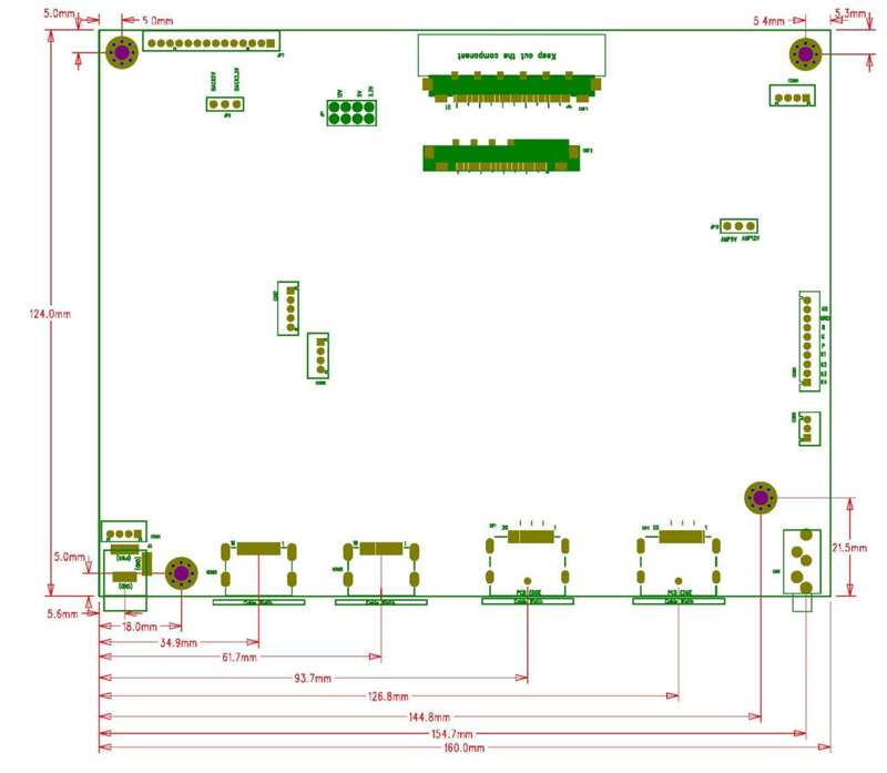
Board Dimension
Board Dimension :160mm*124mm
Screw holes*4:3.0mm
 Download